Scalable ion traps
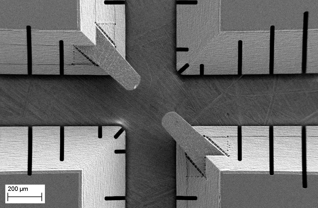
We are developing a cryogenic apparatus similar to that used in the LogiQ project for testing technologies which will aid us in producing ion traps with higher levels of complexity and control suitable to scaling to 100s of ions. On the one hand, we take advantage of laser-assisted chemical etching to make precisely machined 3-dimensional traps with wafer-wafer self-alignment at the micron level. This allows us to investigate more flexible designs than used previously for 2-dimensional junctions in a trap array. This trap will have approx. 150 electrodes and be capable of storing ions in multiple regions simultaneously. A picture of some of the machined wafers is shown below.
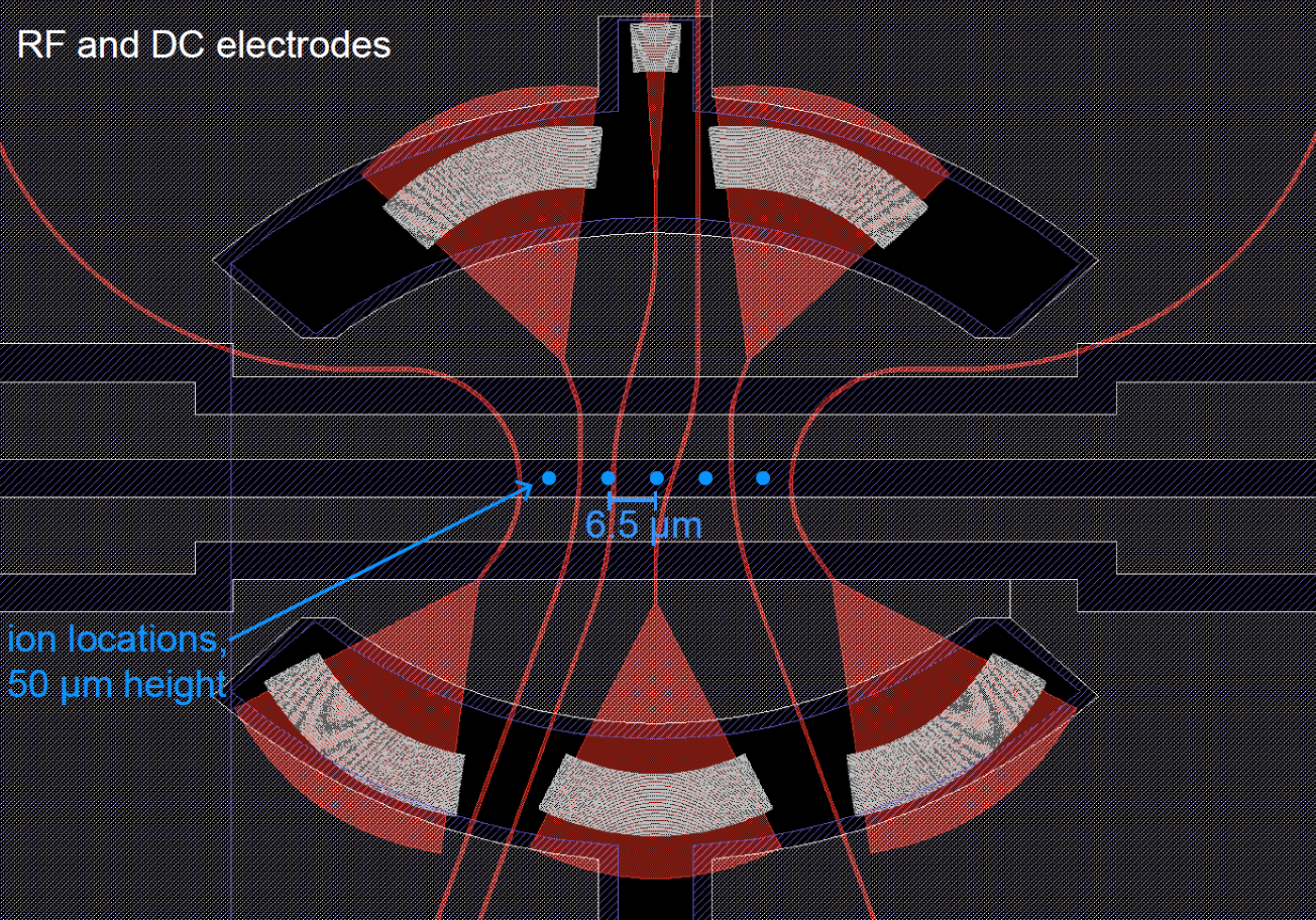
The second area of investigation is the development of surface-electrode traps with integrated SiN photonics. We have developed several new designs optimized for various features, including 5-ion arrays with individual addressing and a trap with integrated optical delivery for fast multi-qubit quantum gates. A drawing of one of these traps is shown below.
With partners at Infineon, Innsbruck, and IFEVS, we are contributing to the development of CMOS-compatible MEMS-fabricated ion traps (PIEDMONS). The project involves design, fabrication, and ultimate testing of 3D multi-metal-layer ion traps in a cryogenic apparatus. Such devices could be robustly produced in a commercial fabrication environment and incorporate exciting new technologies like low-noise, cryogenic generation of control signals, automated calibration routines, and more. Development of these technologies could prove valuable for scaling ion trap systems for quantum computing."
This work is supported by external grants from the EU and the SNF.